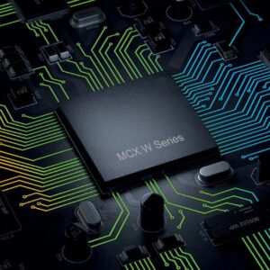
描述
| Category | Details |
|---|---|
| Application Core | – Arm Cortex – M33 core up to 96MHz – 1MB program flash with ECC – 128kB SRAM – Nested Vectored Interrupt Controller (NVIC) – Wakeup Interrupt Controller (WIC) |
| Wireless Module Core | – Dedicated CM3 core – Secure 256kB flash for validated NXP 15.4 and BLE controller stack firmware – 88kB dedicated SRAM – Wireless module compliant with IEEE 802.15.4–2015 – 101dBm 250kbps receive sensitivity – Enhanced ACK timing support in 802.15.4 hardware – Dual PAN support – 2.4GHz Bluetooth Low Energy (BLE) V5.3 upgradable wireless module supports up to 24 concurrent hardware connections in any master/slave combination – –106dBm 125kbps long – range receive sensitivity – –102dBm 500kbps long – range receive sensitivity – –97.5dBm 1Mbps receive sensitivity – –95dBm 2Mbps receive sensitivity – Programmable transmit output power up to +10dBm – Data rates: 125kbps, 500kbps, 1Mbps, 2Mbps – Modulation types: 2 – level FSK, GFSK, MSK, GMSK – On – chip balun with single – ended bidirectional RF port |
| EdgeLock Secure Region | – Secure boot and debug – Symmetric key encryption—AES – 128/192/256 and ECB, CBC, CTR, GCM, CMAC, CCM modes – Asymmetric key encryption—ECC NIST P–192/224/256/384/521, Curve25519 – Key exchange algorithms—ECDH(E), SPAKE2+, JPAKE – Secure key generation, storage, and management – Flash access protection and optional on – the – fly decryption using PRINCE XEX block cipher mode |
| Low Power | – Transceiver current (DC – DC buck mode, 3.3V supply) – Typical RX current: 4.7mA – Typical TX current: 4.6mA at 0dBm, 18.7mA at 10dBm – Multiple power – down modes supporting currents as low as 300nA – Ultra – low – power smart power switch, sleep current < 100nA, wakeup from internal timer or GPIO |
| Clocks | – Supports 26MHz and 32MHz with BLE and Generic FSK modes – 32.768kHz crystal, optional for BLE communication |
| Operating Characteristics | – Ambient temperature range: −40°C to 105°C – Temperature range (junction): – 40°C to 125°C – DC/DC voltage range: 1.8V to 3.6V – Bypass voltage range: 1.8V to 3.6V – Certification: AEC – Q100 Grade 2 |
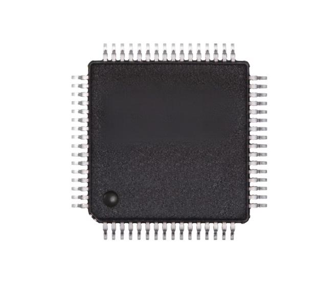
| Human – Machine Interface | 29 GPIO (48HVQFN) |
| System Peripherals | – DC – DC converter supporting buck and bypass operation modes – Asynchronous DMA controller with per – channel access rights (secure/non – secure) – Wakeup unit for power – down modes |
| Analog Modules | – 16 – bit single – ended SAR analog – to – digital converter (ADC) up to 2Msps – Two high – speed analog comparators (CMP) with 8 – bit digital – to – analog converter (DAC) – 1.0V to 2.1V voltage reference (Vref) – Nested Vectored Interrupt Controller (NVIC) – Wakeup Interrupt Controller (WIC) |
| Timers | – Two 6 – channel 32 – bit timers (TPM) with PWM function, support DMA – Two 32 – bit low – power timers (LPTMR) or pulse counters with compare function – 4 – channel 32 – bit low – power periodic interrupt timer (LPIT), support DMA – One 56 – bit timestamp timer – 32 – bit second real – time counter (RTC) with 32 – bit alarm and independent power supply – Signal Frequency Analyzer (SFA) provides devices for measuring clock cycles/frequencies and trigger intervals |
| Communication Interfaces | – Two low – power UART (LPUART) modules – Two low – power SPI modules and one MIPI – I3C module – Two low – power I²C (LPI2C) modules supporting System Management Bus (SMBus) specification version 2 – One programmable FlexIO module supporting emulation of UART, I²C, SPI, camera IF, LCD RGB, PWM/waveform generation |

评价
目前还没有评价